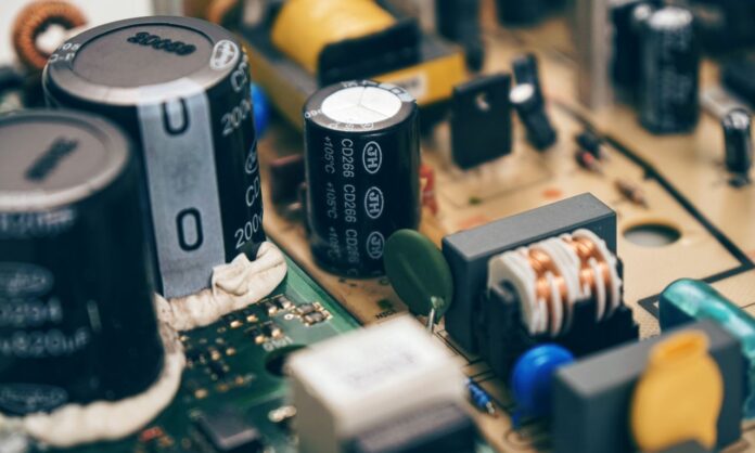

As electronic devices become faster and more advanced, PCB performance has become essential for reliable operation across industries such as automotive, healthcare, telecommunications, and automation. High-speed applications require more than component connections; they depend on strong signal integrity. Poor signal quality can cause data errors, interference, and system failures. Therefore, effective circuit board design plays a vital role in creating efficient, stable, and high-performing electronic systems.
This blog explores why PCB signal integrity matters, the common challenges engineers face, and the practical solutions that help ensure reliable high-speed performance.
Understanding PCB Signal Integrity
Signal integrity refers to the quality and reliability of electrical signals as they travel across a printed circuit board. In an ideal scenario, every signal reaches its destination without distortion, delay, or interference. However, as operating speeds increase, maintaining clean signal transmission becomes much more challenging.
Even minor design flaws can create problems such as reflections, crosstalk, impedance mismatches, and timing errors. These issues may not be noticeable in low-speed electronics, but they can significantly impact high-speed systems where data travels at extremely fast rates.
Effective PCB board design focuses on minimizing these issues from the beginning of the development process rather than attempting to correct them after manufacturing.
Why Signal Integrity Matters in High-Speed Applications
Modern electronic products rely on fast communication between processors, memory, sensors, and communication interfaces. As signal frequencies continue to increase, PCB layout becomes increasingly important.
Strong signal integrity provides several benefits, including:
- Reliable high-speed data transfer
- Reduced communication errors
- Improved device stability
- Better electromagnetic compatibility
- Lower power consumption
- Enhanced product reliability
- Longer operational lifespan
Without proper planning, even a high-quality custom circuit board may fail to meet performance expectations due to poor signal quality.
Common Signal Integrity Challenges
Designing high-speed PCBs requires engineers to overcome multiple technical challenges. Understanding these issues helps developers build more reliable products.
Impedance Mismatch
Every signal path has a characteristic impedance. If traces, connectors, or components have inconsistent impedance values, part of the signal reflects back toward its source instead of continuing forward.
These reflections can distort signals and reduce communication accuracy. Careful PCB board design ensures impedance remains consistent throughout critical signal paths.
Crosstalk Between Signal Lines
When traces carrying high-speed signals are placed too close together, electromagnetic fields from one trace can interfere with another.
This phenomenon, known as crosstalk, introduces unwanted noise that may result in communication errors or unstable system performance.
Proper spacing, optimized routing, and strategic layer placement help reduce crosstalk in a custom circuit board.
Signal Reflection
Reflections occur when signals encounter sudden changes in impedance or poorly designed routing paths. Reflected signals interfere with incoming signals, creating waveform distortion.
Designing controlled transmission lines and minimizing abrupt routing changes significantly improve signal quality.
Electromagnetic Interference (EMI)
High-speed circuits naturally generate electromagnetic radiation. If not managed properly, EMI can interfere with nearby circuits and reduce overall product reliability.
Good PCB layouts, effective grounding strategies, and shielding techniques help minimize electromagnetic emissions.
Timing Skew
Many digital systems require multiple signals to arrive simultaneously. Unequal trace lengths can create timing differences that lead to synchronization problems.
Length matching is an essential practice during PCB board design, especially for high-speed memory interfaces and communication buses.
Factors That Influence Signal Integrity
Several design decisions directly affect PCB signal performance.
PCB Stack-Up Design
The arrangement of conductive and insulating layers influences impedance, grounding, and signal routing.
A carefully planned stack-up provides controlled impedance while reducing interference between signal layers.
Trace Width and Routing
Signal traces should maintain consistent width throughout the design. Sudden width changes alter impedance and increase the likelihood of reflections.
Smooth routing with fewer sharp corners also contributes to better signal transmission.
Ground Plane Design
Continuous ground planes provide stable return paths for electrical signals. Interrupted or fragmented ground planes increase noise and reduce signal quality.
Proper grounding remains one of the most effective methods for improving signal integrity.
Component Placement
Strategic placement minimizes signal travel distance and reduces routing complexity.
High-speed components should remain close together whenever possible to shorten signal paths and improve reliability.
Practical Solutions for Better PCB Signal Integrity
Achieving excellent signal integrity requires a combination of engineering expertise, simulation tools, and manufacturing precision.
Controlled Impedance Routing
Maintaining consistent impedance throughout high-speed traces reduces reflections and improves communication reliability.
Simulation software helps engineers calculate optimal trace dimensions before manufacturing begins.
Differential Pair Routing
Many modern interfaces use differential signals to improve noise immunity.
Routing differential pairs with equal lengths and consistent spacing helps maintain balanced signal transmission throughout the custom PCB board.
Proper Layer Management
Separating high-speed, analog, digital, and power signals across dedicated PCB layers minimizes interference.
Well-organized layer assignments improve both signal quality and electromagnetic compatibility.
Power Distribution Optimization
Stable power delivery directly influences signal integrity.
Proper decoupling capacitors, optimized power planes, and low-noise voltage distribution help maintain consistent performance under varying operating conditions.
Advanced Simulation and Analysis
Modern PCB development includes simulation before manufacturing.
Engineers analyze impedance, signal timing, electromagnetic behavior, and thermal performance to identify potential problems early.
These simulations reduce redesign costs while improving product reliability.
The Role of Embedded Systems in PCB Performance
Hardware and software work together in modern electronics. High-speed PCBs are often integrated into intelligent embedded platforms that control communication, processing, sensing, and automation.
An experienced embedded system company understands how firmware, hardware architecture, processors, memory interfaces, and PCB layouts interact during product development.
This integrated approach allows engineers to optimize overall system performance instead of focusing only on individual hardware components.
By combining embedded expertise with advanced PCB engineering, organizations can create products that perform reliably even in demanding environments.
Conclusion
Signal integrity plays a vital role in ensuring reliable performance, speed, and accuracy in modern electronic systems. Effective circuit board design, optimized layouts, and advanced testing methods help overcome high-speed PCB challenges. By combining high-quality custom circuit board development with the expertise of an experienced embedded systems company, businesses can create efficient, stable, and future-ready electronic products that meet evolving technological demands.
With advanced technology expertise and a commitment to engineering excellence, Tessolve delivers end-to-end semiconductor and electronics solutions, supporting chip design, product development, and system innovation. Its services include PCB board design, custom circuit board development, embedded software, hardware engineering, validation, testing, ASIC design, FPGA solutions, and product engineering. Tessolve helps businesses create reliable, high-performance embedded and semiconductor products for diverse industry applications.
READ ALSO: How Modern LED Strip Systems Are Improving Flexible Lighting Design